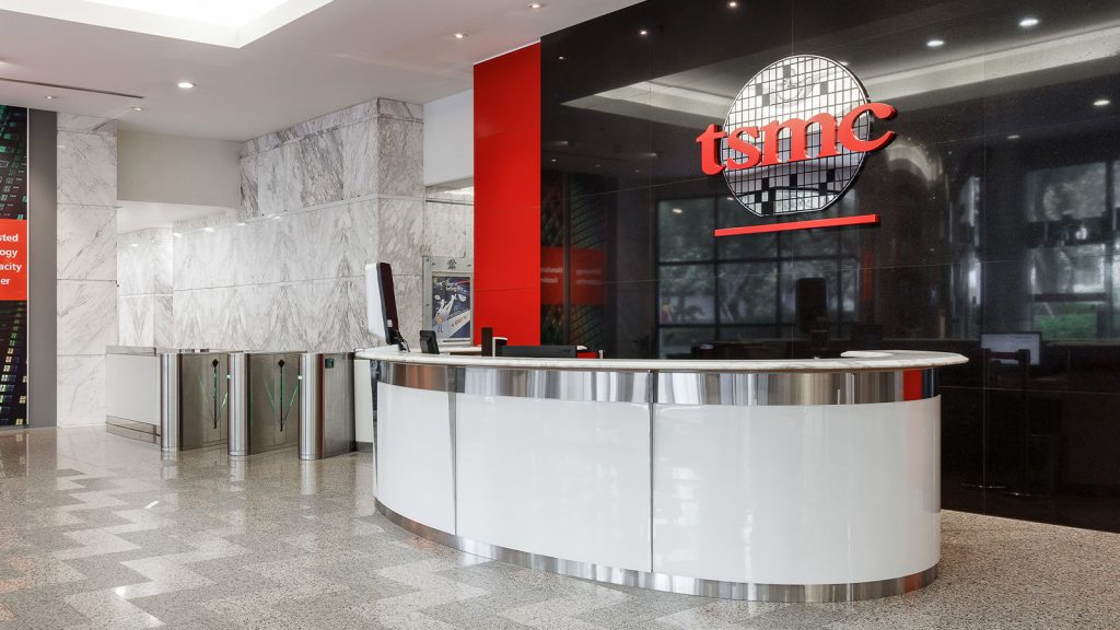
In a significant move poised to bolster Europe’s semiconductor landscape, Taiwan Semiconductor Manufacturing Company (TSMC) has announced the opening of its first chip design center in Munich, Germany. The announcement was made during the European Technology Symposium held in Amsterdam, marking a pivotal moment for both TSMC and the European chip industry.
Purpose and Functionality of the Munich Design Center
The Munich facility is set to play a multi-faceted role in enhancing the capabilities of local and European chip developers. It will assist in optimizing designs for TSMC’s process technology, a critical step in the chip development process. This center aims to bridge the gap between product design and manufacturing, a crucial aspect considering the increasing complexity of chip designs in various applications.
As Kevin Zhang, Deputy Co-COO and Senior Vice President of Business Development and Global Sales, emphasized during the symposium, the facility will not only support fundamental design efforts for microcontroller units (MCUs) tailored for the automotive sector but also focus on advanced design technology optimization (DTCO) for high-performance computing (HPC) and artificial intelligence (AI) applications. The center will bring together expertise that spans the spectrum of design needs, from simple integrations to sophisticated, cutting-edge processor architecture.
Significance of TSMC’s Expansion into Europe
The Munich design center will be TSMC’s 10th such facility globally, and notably, the first in Europe. This development underscores the revitalization of the European semiconductor sector, an area that has faced challenges in maintaining competitiveness against dominant players in Asia and North America. TSMC currently operates nine design centers across various countries, including Canada, China, Japan, Taiwan, and the United States, suggesting a well-established international presence.
Furthermore, TSMC’s establishment of this design center aligns with broader industry trends. In recent years, there has been a concerted effort to enhance Europe’s semiconductor capabilities, especially in light of shifting geopolitical dynamics and supply chain vulnerabilities exposed by the COVID-19 pandemic. In fact, the European Commission is targeting the semiconductor segment to account for 20% of global chip production by 2030, up from the current 10% [European Commission](https://ec.europa.eu/info/news/achieving-eus-2030-goals-semiconductors-2021-nov-11_en).
Collaboration with Industry Giants
TSMC’s design center in Munich is not just an isolated effort but is part of a larger initiative involving well-known industry players, including Bosch, Infineon, and NXP. Together, they are working on the construction of a semiconductor fabrication plant focused on MCUs, which will utilize TSMC’s cutting-edge N12 and N16 process nodes. This collaborative approach aims to address the growing demand for sophisticated chips in a variety of applications, particularly in the automotive sector where reliable and efficient microcontrollers are paramount.
As TSMC continues to integrate closely with its clients, Zhang noted, “It is not like you bring the technology there and you can do manufacturing for the rest of your life. You need to work closely with your end customer to continue to make an improvement.” This philosophy reflects TSMC’s commitment to not merely provide manufacturing services, but to cultivate a collaborative ecosystem that leverages local expertise and fosters innovation.
Market Impact and Future Prospects
The establishment of this design center is expected to have a ripple effect throughout the European chip market. By enhancing local design capabilities, TSMC is positioning itself as a key player in a region eager to regain its foothold in semiconductor manufacturing. The center’s focus on advanced optimization techniques is particularly crucial, as contemporary chips require design efficiencies that transcend traditional Electronic Design Automation (EDA) tools.
Additionally, TSMC’s Munich facility could catalyze further investments from other semiconductor firms, encouraging a more robust ecosystem in Europe. The move to set up a design center also signals TSMC’s longer-term strategy to diversify its manufacturing and design footprint amid increasing global competition for semiconductor dominance [Reuters](https://www.reuters.com/technology/exclusive-tsmc-accelerates-european-expansion-2021-11-10/).
Conclusion
As the semiconductor industry continues to evolve rapidly, TSMC’s Munich design center exemplifies a crucial step for both the company and the European tech landscape. The facility stands to not only enhance local design capabilities but also contribute to a more resilient and self-sufficient semiconductor ecosystem in Europe. With increasing collaboration among major industry players, the future prospects for the region’s chip development appear promising, paving the way for innovations that could reshape technology as we know it.
Quick Reference Table
| Facility | Location | Function |
|---|---|---|
| Chip Design Center | Munich, Germany | Supports local chip development and optimization |
| Global Design Centers | Various Locations | Assists in chip design and technology co-optimization |
| Collaborators | Various Firms | Mainly Bosch, Infineon, NXP |
| New Fab Details | In progress | Focus on MCUs using N12 and N16 processes |
| European Commission Goal | By 2030 | 20% market share in global semiconductor production |

